3D keyboard wiring
From DMOTE application configuration to QMK firmware code
This article describes my thought process in one stage of computer keyboard design. It is not a build guide, nor a manual for the DMOTE application or the QMK firmware project, but it describes a concrete example of a bridge all the way from CAD to figuring out and encoding the wiring of switches to a microcontroller.
There has been a time that technical considerations exerted a very strong pressure towards minimization of the number of flip-flops used and to use more than six flip-flops to build a finite-state machine with at most 64 states was at that time regarded, if not as a crime, at least as a failure.— Edsger W. Dijkstra, A Discipline of Programming (1976)
Wiring up a newly designed 3D keyboard is like sewing. When you sew a garment, you’re usually working on it inside out. To plan for a good fit, you must be able to map two-dimensional cloth to a three-dimensional wearer’s body, constantly everting the garment in your mind. It is the same with ergonomic electronics: A series of transformations in your hands and in your head.
Contents
Overview
This article uses the first Concertina as a case study to describe the middle part of the following procedure.
- Figure out what keys you want.
- Design physical matrices as part of the case.
- Print the case and insert the switches.
- Design the logical matrix. ← Main subject of this article.
- Solder wires and diodes in place.
- Encode the logical matrix in firmware.
- Flash and test firmware.
Physical shape
The Concertina, our example project for this article, has its main key clusters on the short ends of a long, blocky shape. On top, it has perpendicular key clusters for your thumbs.
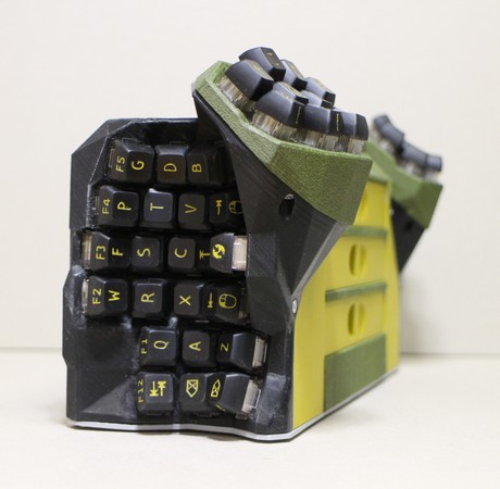
The four key clusters are not flat, nor would a linear projection of them all onto a single plane be all you need in deciding how to wire up the interior. Thus normal two-dimensional planning for wiring would be inadequate.
CAD specification
The Concertina’s shape is determined by configuration parameters to the DMOTE application, a keyboard CAD program. Here follows an excerpt from a YAML configuration file that is bundled with version 0.6.0 of that application. Irrelevant sections of the file are omitted.
key-clusters:
  main:
    [---]
    matrix-columns:
    - rows-above-home: 1
      rows-below-home: 1
    - rows-above-home: 1
      rows-below-home: 2
    - rows-above-home: 1
      rows-below-home: 3
    - rows-above-home: 1
      rows-below-home: 2
    - rows-below-home: 2
    - rows-below-home: 2
    [---]
  thumb0:
    [---]
    matrix-columns:
    - rows-above-home: 1
    - rows-above-home: 1
      rows-below-home: 1
    - rows-above-home: 1
      rows-below-home: 1
    - rows-above-home: 1
That is from the Concertina’s base.yaml, describing the right-hand side of the keyboard case. The same configuration file also specifies that the two key clusters (main and thumb0) should be mirrored on the other side of the keyboard case, which is the left-hand side, as seen in the photos. The excerpt thus describes all four key clusters. Disregarding the final shape for the moment, the heart of the configuration can be visualized in a grid pattern.
| ◯ | ◯ | ◯ | ◯ | Above home | ◯ | ◯ | ◯ | ◯ |
| ◯ | ◯ | ◯ | ◯ | Home row | ◯ | ◯ | ◯ | ◯ |
| ◯ | ◯ | Below home | ◯ | ◯ |
| ⬤ | ⬤ | ⬤ | ⬤ | Above home | ⬤ | ⬤ | ⬤ | ⬤ | ||||
| ⬤ | ⬤ | ⬤ | ⬤ | ⬤ | ⬤ | Home row | ⬤ | ⬤ | ⬤ | ⬤ | ⬤ | ⬤ |
| ⬤ | ⬤ | ⬤ | ⬤ | ⬤ | ⬤ | Below home | ⬤ | ⬤ | ⬤ | ⬤ | ⬤ | ⬤ |
| ⬤ | ⬤ | ⬤ | ⬤ | ⬤ | ⬤ | ⬤ | ⬤ | ⬤ | ⬤ | |||
| ⬤ | ⬤ |
This tabular visualization is an abstraction, resembling a flat enthusiast keyboard, such as an Iris. It has been adapted only slightly to the actual shape of the case, in that the thumb clusters are shown above the main clusters. I’m using black dots for the main clusters to match the black plastic of the print.
2D visualization
Since this article was first written, the Concertina has been added to the QMK firwmare project. Here is its visual representation in QMK Configurator as of April 2021:
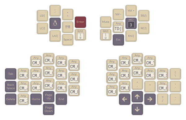
This representation is more concrete than the table above, but still fails to convey the third dimension.
Planning
Here is just the left-hand side’s two key clusters, as seen with soldering iron in hand.
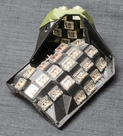
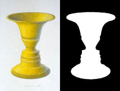
To start moving from this physical object toward a mental model for wiring, I find it helpful to look at the print as something like a Rubin vase: Two different scenes that are in a sense mutually exclusive, yet both obvious and unambiguous in the same object.
Here is the keyboard case again, with an intermediate abstraction superimposed from the tabular visualization of the DMOTE application’s configuration file.
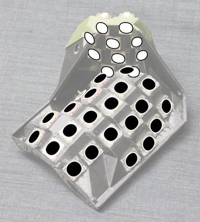
The physical shape and the disconnected mathematical graph of its switches are both valid and necessary ways to look at the same object. The nodes of the graph can be tidied up while maintaining a similar overall shape.
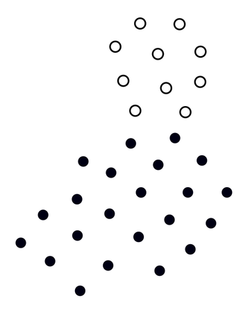
Keeping both the concrete object and this abstraction in mind, you can start sketching how to run the wires. I normally use paper and coloured markers to do this, not vector graphics.
Objectives and parameters
The main requirement in wiring a keyboard is for each node (i.e. switch) to be a unique intersection of exactly one row and one column. Briefly stated, the variables are the number of different wires you use, and how you use them.
The example keyboard in this article has 64 keys in total, a square number that we can factorize most efficiently as 8 × 8. This means that the smallest number of wires you could possibly use is 8 + 8, that is 8 rows and 8 columns, occupying 16 of the MCU’s I/O pins.
For this example project, I had a Pro Micro, the smallest microcontroller board in common use with QMK in 2020. The Pro Micro has 18 easily usable I/O pins, and 2 more that are not so easy. Using 16 pins leaves room to spare for other functionality, such as backlighting or audio.
In this example project, I did not have any such use planned for the spare pins, so I could have gone with a different sort of layout. However, I could not have wired each half of the keyboard to its own set of MCU pins, without sharing any pins between the two halves. 32 switches sharing no pins with the other 32 would have required at least 12 pins, for a sum of 24. That’s too many for one Pro Micro, but other microcontroller boards could have done it, and in a truly split keyboard, there would have been two separate MCUs, easily accomodating more keys. Not sharing pins would have simplified the wiring of the Concertina, albeit only slightly, so it can make sense to buy a bigger board than you really need.
Within the limits of the Pro Micro, I could have gone with a sparse matrix, where not every intersection is occupied. As an extreme example, 12 columns and 8 rows would cover the entire tabular cluster diagram above, and use all 20 I/O pins. The bottom row in such a solution would have contained only two keys, leaving 10 unused or “blank” spots on that row. This would have simplified firmware programming, but it would also have made the wiring unnecessarily difficult in that there would be more wires, run without concern for physical proximity.
To summarize, the parameters at this stage of planning are:
- The choice of MCU.
- Competition over MCU pins.
- Ease of wiring at the switch side (proximity).
- Ease of wiring at the MCU side (sharing).
- Ease of firmware programming for the matrix.
My advice for how to set each parameter is to think long term. Firmware programming is a one-time cost, short of losing your source code. Other costs recur. The overall ease of wiring is a factor in maintenance. Keyboards get dirty, wear out, and must ultimately be recycled. Switches and MCUs may need to be replaced for repair or upgrade. A solution that is rational for assembly can seriously complicate maintenance. When in doubt, keep it simple: Easy to disassemble, inspect and understand, not just easy to make.
Composition
In my Concertina build, I went with a dense matrix of 8 × 8. Here is the final plan for how to wire it up.
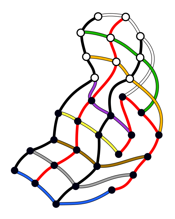
All wires, 10 colours
If that picture is not clear, try these:
One point of interest in this composition is the last row on the right, in red. It appears to loop back on itself where the main key cluster is deepest. More on that later.
Another point of interest is that some of the wires cross. That is not necessary. It would have been possible to connect the main and thumb clusters in such a way that the diagram would have looked better, free of intersections beyond the nodes. For example, the white and orange wires could trade their points of attachment to the main cluster. Again, more on that later.
Physical implementation
Here’s what the left-hand side looks like, wired up according to plan, and helping to make that plan. Diodes are on row legs.
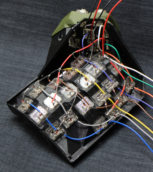
Notice the last row: That second red wire again, on the right. In the abstract diagram, this row looped back on itself, but the physical wire does not. Instead, that row’s diodes lean over to touch a gentle curve that passes between the switches. This is one case where planning with the physical object in hand, and taking even the ancillary components into consideration, can make the solution easier than an abstraction makes it appear.
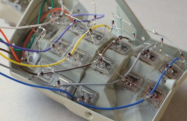
Another unit: diodes linked more directly by their legs
Notice also that each of the 12 wires must leave this part of the case to approach the MCU. In the Concertina, this should be done roughly from where the clusters intersect. The wires that cross in the diagram, as they connect the thumb and main clusters, are anchored at the main cluster to make a bundle with all the other columns, before heading off toward the MCU.
There is an extra length of wire in all of those transitions between the two key clusters. This leeway is designed to facilitate assembly and disassembly. For more detailed pictures of the right-hand side in various stages of wiring, where the extra length is more obvious, see the Concertina v0.6.0 build guide. It would have been possible to achieve this feature with a diagram free of crossing wires, but the orange wire would have had to bend just a little more sharply, adding stress. In this detail, a practical physical body takes priority over a neat diagram.
Firmware implementation
The Concertina build guide has an MCU pinout. More relevant here is the following fragment of firmware (QMK) source code.
#define LAYOUT_64key( \
                  LT_32, LT_22, LT_12,                 RT_12, RT_22, RT_32,               \
                  LT_31, LT_21, LT_11, LT_01,   RT_01, RT_11, RT_21, RT_31,               \
                         LT_20, LT_10, LT_00,   RT_00, RT_10, RT_20,                      \
                                                                                          \
                  LM_34, LM_24, LM_14, LM_04,   RM_04, RM_14, RM_24, RM_34,               \
    LM_53, LM_43, LM_33, LM_23, LM_13, LM_03,   RM_03, RM_13, RM_23, RM_33, RM_43, RM_53, \
    LM_52, LM_42, LM_32, LM_22, LM_12, LM_02,   RM_02, RM_12, RM_22, RM_32, RM_42, RM_52, \
    LM_51, LM_41, LM_31, LM_21, LM_11,                 RM_11, RM_21, RM_31, RM_41, RM_51, \
                         LM_20,                               RM_20                       \
) \
{ \
  { LT_00, LT_10, LT_20, LT_31, LM_20, LM_31, LM_41, LM_51 }, \
  { LT_01, LT_11, LT_21, LM_11, LM_21, LM_32, LM_42, LM_52 }, \
  { LT_12, LT_22, LT_32, LM_12, LM_22, LM_33, LM_43, LM_53 }, \
  { LM_02, LM_03, LM_04, LM_13, LM_23, LM_14, LM_24, LM_34 }, \
  { RT_00, RT_10, RT_20, RT_31, RM_20, RM_31, RM_41, RM_51 }, \
  { RT_01, RT_11, RT_21, RM_11, RM_21, RM_32, RM_42, RM_52 }, \
  { RT_12, RT_22, RT_32, RM_12, RM_22, RM_33, RM_43, RM_53 }, \
  { RM_02, RM_03, RM_04, RM_13, RM_23, RM_14, RM_24, RM_34 }, \
}
This C preprocessor macro acts as a sort of dictionary. It translates a plain-text diagram of the case layout resembling QMK Configurator’s visualization, one key cluster at a time, to the electronic layer, where the four key clusters of the Concertina form one 8 × 8 matrix.
To make this code easier to understand, here’s just the left-hand side, in the black and white of this article’s other diagrams, and with the colours of the wiring (as shown here and here) on the edges.
| White | Green | Orange | Purple | Yellow | Brown | Grey | Blue | |
|---|---|---|---|---|---|---|---|---|
| Black | ◯ LT_00 | ◯ LT_10 | ◯ LT_20 | ◯ LT_31 | ⬤ LM_20 | ⬤ LM_31 | ⬤ LM_41 | ⬤ LM_51 |
| Red | ◯ LT_01 | ◯ LT_11 | ◯ LT_21 | ⬤ LM_11 | ⬤ LM_21 | ⬤ LM_32 | ⬤ LM_42 | ⬤ LM_52 |
| Black | ◯ LT_12 | ◯ LT_22 | ◯ LT_32 | ⬤ LM_12 | ⬤ LM_22 | ⬤ LM_33 | ⬤ LM_43 | ⬤ LM_53 |
| Red | ⬤ LM_02 | ⬤ LM_03 | ⬤ LM_04 | ⬤ LM_13 | ⬤ LM_23 | ⬤ LM_14 | ⬤ LM_24 | ⬤ LM_34 |
Once again, have a look at that last row, at the bottom. The way it’s encoded here, it moves from the first column of the main cluster (LM_0*) to the second (LM_13), to the third (LM_23), and then back to the second, and then it proceeds all the way to the fourth column, per the wiring diagram.
This representation of the last row is a consequence of its illusory loop. It is a physical coincidence that those switches at the edge of the main cluster—the cluster’s first column in DMOTE terms—are most conveniently wired up along a row in QMK, and linked up to the perpendicular edge of the thumb cluster. Just as the CAD representation and the firmware do not need to have the same coordinate system, they don’t really need anything else in common, beyond the number of keys. The preprocessor macro sees to that.
This concludes the bridge from CAD to firmware, and this look at keyboard design. I picked this specific example because the dense matrix and the separation of clusters allow a range of principles to come into play. You can apply the same kind of thinking to a DMOTE, or any keyboard that isn’t flat.